Archive for the ‘emulation’ Category

ISA Bus Sniffer update

Monday, February 8th, 2016

Several years ago, I designed the ISA bus sniffer, a sort of special-purpose logic analyzer for capturing the signals from the CPU and ISA bus in an XT-class system. Well, I finally got around to finishing it, writing the three pieces of software needed to make it work (the microcontroller program, the 8088 test harness and the decoder, as well as making the changes to the XT Server to retrieve traces.

Here is what the contraption looks like:

ISA Bus Sniffer, completed

In this picture you can also see the board that goes into the 8087 FPU socket to probe the CPU pins. The yellow wires go to a switch so that I can remotely reset the microcontroller for reflashing.

Here is how it fits into the machine:

ISA Bus Sniffer in situ

Here is what the XT Server currently looks like:

ISA Bus Sniffer in situ

And here is an example of what the output from the sniffer looks like after decoding:

20FFF .p...  00F24 FF 00 FC .......
20FFF Ip...  00F24 FF 01 FC .......                          I
20FF1 SC...  00F24 FF 01 FC .......  T1                      S F6E1         MUL CL
00F25 .C...  00F25 FF 01 FC .....D.  T2 S0
20F25 .C...  00F25 FF 01 FC .....D.  T3 S1
20F25 .C...  0020B FF 10 FC .....D.  Tw S2
20F25 .C...  0020B FF 10 FC ..r..D.  Tw S3
20F25 .C...  0020B FF 10 FC .Wr..D.  Tw S4 FF <-d [   0020B]
20F25 .C...  0020B FF 00 FC .....D.  Tw
20FFF .C...  00F25 FF 00 FC ..r....  Tw
20FF6 .C...  00F25 F6 00 FC ..r....  Tw
20FF6 .p...  00F25 F6 00 FC ..r....  T4    F6 <-f [   00F25]
20FF6 .C...  00F25 F6 00 FC .......  T1
00F26 .C...  00F26 F6 00 FC .......  T2
20F26 .C...  00F26 FF 00 FC ..r....  T3
20FE1 .p...  00F26 E1 00 FC ..r....  T4    E1 <-f [   00F26]
20FE1 .p...  00F26 E1 00 FC .......

From left to right the columns are: CPU address/data, CPU flags, bus address, bus data, DMA requests and acks, interrupt requests, bus flags, bus states for CPU and DA accesses, transfers, prefetch queue status, instruction data and decoded instruction.

You can try this out! Grab these files:
https://github.com/reenigne/reenigne/blob/master/8088/defaults_bin.asm
https://github.com/reenigne/reenigne/blob/master/8088/defaults_common.asm
https://github.com/reenigne/reenigne/blob/master/8088/trace/trace.asm
http://yasm.tortall.net/Download.html (NASM should work too with minor modifications).

Replace the code under "testRoutine:" with the code that you'd like to get a trace of (it needs to run exactly the same each time it's run, so be sure to initialize all registers and memory you use - I made that mistake and it has me scratching my head for a bit). Build trace.bin and upload it to http://www.reenigne.org/xtserver - within seconds you should get a link to a trace like the one above.

How to get away with disabling DRAM refresh

Monday, October 29th, 2012

On the original IBM PC 5150 (and it's mostly electrically-equivalent derivatives, the 5155 and 5160) the operation of the bus (the data channel between the CPU and it's memory and peripherals) is interrupted is interrupted 2,187,500 times every 33 seconds (a rate of about 66KHz) for 11/13,125,000 of a second each time (i.e. 4 out of every 72 CPU cycles). During that time, very little of the machine can operate - no RAM can be read or written and no peripherals can be accessed (the CPU might be able to continue doing it's thing if it's in the middle of a long calculation, and the peripherals will continue to operate - it's just that nothing can communicate with each other).

Why does this happen? Well, most computers (including the one this blog post is about) use DRAM (Dynamic RAM) chips for their main memory, as it's fast and much cheaper than the slightly faster SRAM (Static RAM) chips. That's because each DRAM bit consists of a single capacitor and transistor as opposed to the 4 or more transistors that make up a bit of SRAM. That capacitor saves a lot of hardware but it has a big disadvantage - it discharges with time. So DRAM cells have to be "refreshed" periodically (every 2ms for the 16 kbit 4116 DRAMs in the original 5150) to maintain their contents. Reading a bit of DRAM involves recharging the capacitor if it's discharged, which refreshes it.

But a computer system won't generally read every bit of RAM in any given interval. In fact, if it's sitting in a tight idle loop it might very well not access most of the memory for many minutes at a time. But we would be justified in complaining if our computers forgot everything in their memories whenever they were left idle! So all general-purpose computers using DRAM will have some kind of circuitry for automatically accessing each memory location periodically to refresh it. In the 5150, this is done by having channel 1 of the 8253 Programmable Interval Timer (PIT) hooked up to the Direct Memory Access (DMA) controller's channel 0. The BIOS ROM programs the PIT for the 66KHz frequency mentioned above, and programs the DMA controller to read a byte each time it's triggered on channel 0. The address it reads counts up from 0 to 65,535 for each access, then goes back down to 0 again.

If the DRAM needs to be refreshed every 2ms why does the refresh circuit run at 66KHz and not 500Hz, or for that matter 8.192MHz? To answer that question, we need to know something about how the memory is organized. The original 5150 had banks of 8 chips (plus a 9th for parity checking). Each chip is 16 kbit, so a bank is 16KBytes. If you had a full 640KB of RAM organized this way, that would be 40 banks or 360 separate chips! (By the time that much memory become common, we were mostly using 64 kbit chips though.) Within each chip, the 16 kbits are organized in a grid of 128 "rows" and 128 "columns". To read a bit, you input the "row" address, then the "column" address, then read back the result (hence the chips could have just 16 pins each, as each address pin corresponds to both a "row" bit and a "column" bit). Happily, whenever a row is accessed, all the DRAM cells on that row are refreshed no matter what column address is ultimately accessed. Also, the low 7 bits of the physical byte address correspond to rows and the next 7 bits correspond to columns (the remaining 6 bits correspond to the bank address). So actually you could quite happily get away with just refreshing addresses 0-127 instead of addresses 0-65,535 on this machine (though there was a good reason for doing so, as we'll see later).

To ensure that they meet tolerances, electronic components (including DRAM chips) are manufactured with certain margins of error, which means that often one could get away with reprogramming the PIT to reduce the DRAM refresh rate a bit in order to squeeze a little bit more performance out of these old machines - it was a common hack to try, and I remember trying it on the family computer (an Amstrad PC1512) after reading a little bit about DRAM refresh in a computer magazine. I seem to recall that I got it up from the standard 1/18 to maybe 1/19 or 1/20 before it became unstable, but the performance improvement was too small to notice, so the little .COM file I made with DEBUG never made it as far as my AUTOEXEC.BAT.

For many of the timing experiments and tight loops I've been playing with on my XT, I've been disabling DRAM refresh altogether. This squeezes out a bit more performance which is nice but more importantly it makes the timings much more consistent (which is essential for anything involving lockstep). However, whenever I've told people about this the reaction is "doesn't that make the machine crash?" The answer is "no, it doesn't - if you're careful". If you turn off the refresh circuitry altogether you have to be sure that the program you're running accesses each DRAM row itself, which happens automatically if you're scanning through consecutive areas of RAM at a rate of more than 66KB/s, or for that matter if you've done enough loop unrolling that your inner loop covers more than 127 consecutive bytes of code. Since these old machines don't have caches as such, unrolled loops are almost always faster than rolled up ones anyway, so that's not such a great hardship.

Not all of the machines I'm tinkering with use 4116 DRAM chips. Later (64KB-256KB) 5150 motherboards and XTs use 4164 (64 kbit) chips, and modified machines (and possibly also clones) use 41256 (256 kbit) chips. The principles are exactly the same except these denser chips are arranged as 256x256 and 512x512 bits respectively, which means that there are 8 or 9 row bits, which means that instead of accessing 128 consecutive bytes every 2ms you have to access 256 consecutive bytes every 4ms or 512 consecutive bytes every 8ms respectively (the PIT and DMA settings were kept the same for maximum compatibility - fortunately the higher density DRAMs decay more slowly so this is possible). So when disabling DRAM refresh, one should be sure to access 512 consecutive bytes every 8ms since this will work for all 3 DRAM types.

The cycle-exact emulator I'm writing will be able to keep track of how long it's been since each DRAM row has been refreshed and will emit a warning if a row is unrefreshed for too long and decays. That will catch DRAM refresh problems that are missed due to the margins of error in real hardware, and also problems affecting only 41256 chips (my machine uses 4164s).

Modern PCs still use DRAM, and still have refresh cycles, though the overhead has gone down by an order of magnitude and the exact mechanisms have changed a few times over the years.

Improved composite mode support for DOSBox

Sunday, October 7th, 2012

I recently contributed to a DOSBox patch to make composite output work in all CGA graphics modes. Most CGA composite games use BIOS mode 6 (port 0x3d8 value 0x1a, aka 640x200 1bpp mode) which gives a nice range of colours. However, there are a rare few games which use a 2bpp mode but have 3.57MHz vertical lines which are quite obviously designed to yield a different palette on the composite output. DOSBox currently shows the output of such games as they would appear on a digital (aka TTL or RGBI) monitor, which isn't always what the game author intended - the example that started the thread was Fooblitsky.

I had already written code to simulate composite CGA in 2bpp mode (and indeed all modes) but there is a complication - DOSBox is based around a 256 colour palette and my code assumes 24-bit colour. The first 16 colours are also reserved for the digital CGA colours so that the palette entries don't have to be reloaded when switching between composite and digital, so only 240 colours can be used for composite CGA. The current DOSBox CGA composite implementation uses 80 palette entries - 16 colours (one for each bit pattern) times 5 brightness levels (0, 1, 2, 3 or 4 pixels lit). I realized that actually only 16 of these palette entries are really needed, since the same information is being used to dereference both the "bit pattern" table and the "brightness" table. Also, DOSBox's current implementation isn't quite right since some of the colour fringes are desaturated - look at the top tapper screenshot (the one from DOSBox) here and compare it to the more correct version below - look in particular at the middle of the "SODA" sign in the window, the right edge of the D and the left edge of the O, which is grey in DOSBox (missing its fringing entirely). Since DOSBox uses a (1, 1, 1, 1) kernel for its NTSC filter, there are only actually 16 possible colour combinations (though they are permutated depending on the colour carrier phase).

I realized that a similar technique might be possible for the 2bpp modes. Each output composite pixel depends on the colours of four consecutive pixels of hdot width. These pixels cover at most 3 consecutive ldots, so any given pixel position depends on at most 6 bits of video data. It also depends on 2 bits of x position, so we need 8 bits of palette entries, or 256 colours - just slightly too many. There's an easy way to reduce the amount of palette entries though - half of the output hdots depend on only 2 consecutive ldots (since the sampled hdots exactly cover 2 ldots). So even hdots have 16 possible colours and odd hdots have 64, for a total of 16+64+16+64 = 160 colours - plenty to spare. What's more, the "render" part of the new algorithm is even faster than it used to be (although the mode setting part is probably much slower - however it's run sufficiently rarely that there's no need to optimize it).

ISA bus sniffer

Friday, October 5th, 2012

One of the trickiest parts of writing my cycle exact 8088 emulator is going to be figuring out exactly when each part of each instruction is executed - in particular, at what point during each instruction's execution is each of its bytes removed from the prefetch queue? And (for instructions which do IO) at which points during the execution are those IO requests sent from the Execution Unit to the Bus Interface Unit?

I was originally thinking that I would have to devise a clever set of experiments to find out - make a hypothesis about the timings, devise an experiment which behaved differently depending on whether that hypothesis was true or not (existence proof: if such an experiment were not possible I wouldn't care about the result for emulation purposes), rinse and repeat until the observed behavior of the emulator stops deviating from the observed behavior of the actual machine.

However, I have learned that there is a easier way to go about it. It turns out that the CPU outputs a couple of bits of information concerning the state of the prefetch queue on two of its pins (QS0 and QS1), allowing us to distinguish between 4 possible operations which can occur on each cycle: first byte of opcode removed, subsequent byte of opcode removed, queue emptied and no change. Being able to read that information (along with exactly what the bus is doing) would make figuring all this out much easier. I didn't want to use a logic probe to do this because (among other reasons) I wanted to be able to set up a large number of experiments and run them all automatically. So instead I have designed an ISA card which (completely transparently to the PC or XT it's plugged into) uses a microcontroller to sample the state of many lines and transmit the results to another PC over a serial connection.

Compared to a real logic probe we can only sample a few lines at once, only gather a couple of KB of samples at once and can't sample very often (I think 4.77MHz should be possible), but the experiments I care about are all deterministic so we can just repeat the experiment enough times to gather all the data I want. Here's the schematic for the bus sniffer and here's what the board layout looks like:

I've ordered a PCB from BatchPCB (the first time I've actually had a PCB professionally made) so we'll see how it works!

Adventures in CRTC lockstep

Monday, October 1st, 2012

Once I had achieved CGA lockstep, I tried some test programs. This image was made by cycling through the possible palette registers as quickly as possible (i.e. it's running a big unrolled loop of "INC AX; OUT DX,AL" to the palette register):

That worked great, except that in making it I noticed that the pattern wasn't always starting the same way - half the time the first visible scanline had different set of colours. Somehow a bit of state was leaking through my lockstep routine!

After a while I figured out that it was due to the way I was getting the CRTC into lockstep with the CGA and CPU. The smallest frame that the 6845 CRTC can do is two character clocks (1 character by 2 scanlines - a 1 scanline high frame doesn't work with that CRTC). I thought I could get around this by going into high-res mode - then 1 character clock is 1 hchar so a frame would be 1 lchar and we'd be in a known place in the frame once we were in a known place in the CGA cycle.

Have you spotted the problem yet? The problem is that I don't know what the phase relationship is between the CGA clock and the CRTC clock - the first hchar of the frame could be the left or the right hchar within the lchar! And in fact, which it turned out to be was decided at random on startup.

With a bit of fiddling I eventually came up with a way to get the CRTC into lockstep as well. The trick hinges on the fact that if we set up the CRTC parameters so that one of the scanlines is displaying a normal visible image and one is overscan, we can tell which scanline is which by reading the display enable bit of the CGA status register. Then we delay an odd number of lchars if the display enable bit is set one way and an even number of lchars if it's set the other way (it doesn't matter which is which). Because we want to keep the CGA and CPU in lockstep as well, the difference in the codepath lengths must also be a multiple of 3 lchars, so delaying for X lchars one way and X+3 the other works fine.

That's about all there is to it. The full lockstep routine is on github. Once lockstep is entered it'll persist until you wait for a time that depends on an external event (such as reading from disk/serial/parallel/ethernet/joystick or waiting for a keystroke). That doesn't mean that lockstep mode games and trackmos are impossible, though. The keyboard can be read by polling (pretty much all PC software directly or indirectly uses an interrupt for keyboard access but it isn't compulsary and I've done it by polling a few times). You just have to make sure the code paths are the same length no matter whether a key was pressed or not and no matter which key was pressed if there is one, which can be done by adding suitable delays. Disk access is a bit more difficult, since there's going to be a DMA bus access at some unpredictable point, and after it's happened you'll be out of lockstep. I think the solution is to HLT after the disk access is complete and restart execution on a timer interrupt. In the event that lockstep between CGA and PIT isn't possible, regaining lockstep once the timer interrupt has occurred should be possible by delaying for N ccycles for some N between 0 and 15 and a CGA memory access. Another possible way is to make sure the CPU is running code that is either:

  1. BIU-bound with no wait states, or
  2. that is EU-bound and never exhausts the prefetch queue

for the entire time that the accesses might be happening. That way the time taken to run the code doesn't depend on exactly when the accesses occur.

Adventures in CGA lockstep

Sunday, September 30th, 2012

As part of my project to emulate an IBM PC or XT with cycle accuracy, I need to be able to get the machine into a completely known and consistent state, which I call lockstep. That way I can run a program many times and be sure of getting exactly the same result each time.

This is a bit tricky, because while all the PC's clocks are derived from a single 14.318MHz crystal, they divide it in different ways. The CPU clock is made by dividing this frequency by 3, the PIT clock is made by dividing it by 4 and the CGA clock is made by dividing it by 16.

Getting the CPU clock in lockstep with the CGA clock is the difficult bit, since the CGA clock is in lockstep with the PIT clock by definition (assuming that such a lockstep is possible - I'm not sure offhand if the phase relationship between the PIT and the CGA clock is always the same or if it's randomized on startup - the latter would make it more complicated to use the PIT in lockstep mode, but that's not really a big problem since the point of lockstep mode is to be able to do timing statically).

Since the CGA clock and the CPU clock have periods which are relatively prime numbers of hdots, it's definitely possible to get them into lockstep. Once I had a rough idea of what the CGA wait states were, I realized that achieving lockstep ought to be possible with a combination of delays and CGA accesses. The algorithm would be:

  1. Do a CGA memory access, reducing the number of possible relative phases from 16 to 3.
  2. Delay for A ccycles.
  3. Do a CGA memory access, reducing the number of possible relative phases from 3 to 2.
  4. Delay for B ccycles.
  5. Do a CGA memory access, reducing the number of possible relative phases from 2 to 1.

Delaying for 16 ccycles gives the same relative phases as delaying for 0 ccycles, so the problem boils down to finding A mod 16 and B mod 16. That's only 256 possibilities (and probably quite a few of those will work) so trial and error works fine. Delaying for particular numbers of cycles is okay too - the 8-bit MUL instruction takes 69 ccycles plus 1 ccycle for each set bit in AL, so as long as you don't mind waiting for 69 ccycles you can get a delay of any number of ccycles you like.

But there's a more fundamental problem - how do we recognize when we've succeeded? The definition of lockstep involves consistency - ending up in a known end state no matter what the initial state. So in order to determine whether we're in lockstep or not, we really need to be able to control the initial state - in other words, in order to figure out whether we're in lockstep or not we first need to be in lockstep! That's a bit of a chicken-and-egg problem.

If I knew exactly what the CGA wait states were at this stage I could have figured out the right A and B values on purely theoretical principles, but I didn't - my examinations of the CGA schematics left some questions (particularly in areas involving how the 8088 treats READY signals occuring at different clock phases, and how some apparent race conditions actually turn out in real hardware). It was only in the course of achieving lockstep that I discovered what the CGA wait states actually are.

I had a few false starts involving identifying the 6 behavior classes for the 27 possible transition tables involved in the long-term behaviors of repeated sections of code. For example, if a piece of repeated code has 3 possible long-term behaviors depending on the relative phase at the start, I know that the repeated section must leave the relative phase alone.

But that was getting rather complicated, and I wasn't really getting anywhere until I hit on a better way - I realized that I could visualize exactly how long a piece of code was taking by running it and then changing the CGA palette register, which has an immediate effect, so marks the position on the screen where the electron beam was pointing when the register changed.

That's only useful if the transition happens in exactly the same place on the screen in each frame (otherwise you don't get a stable image and can't see what's going on). Which sounds like we're back to the chicken-and-egg problem again. But it's a more limited kind of lockstep that we need for this particular experiment - we don't need absolute lockstep, just a way of getting code to run at a consistent place relative to the raster beam, from frame to frame. That is to say, it doesn't matter if next time we run the program the image appears in a different place on the screen.

Fortunately, there's a way to do this on the PC even if we don't have full lockstep, since we can use the PIT to introduce a lockstep that's just consistent from frame-to-frame, not from run-to-run. If we set a timer to go off exactly 262*912/12 = 19912 PIT cycles, it'll occur exactly once every frame. That's not quite enough though, because interrupts don't quite have an instantaneous effect on the CPU - the CPU does finish whatever instruction it's currently executing before starting an interrupt. So you have to make sure it's not executing any instructions - i.e. is in the halt state. Another complication is that I had to disable all other interrupts and the DRAM refresh in order to avoid them messing up the timings, which meant that I had to access each DRAM row within a certain period of time lest the capacitors discharge and the memory contents decay, which meant that I couldn't leave the CPU halted for too long!

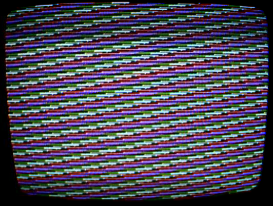
Once I had a stable image I was able to generate the 16 different CGA/CPU relative phases with multiply instructions, and made a diagonal line that advanced 3 hdots (1 ccycle) on each line just by cycle counting. Then by placing CGA memory accesses between this diagonal line and the palette write I was able to see exactly what the CGA wait states were:

It look a while to get this image because whenever I added some code to a line I had to change the delay code at the end of the line to get the start of the next line to line up correctly, so there was a fair amount of trial and error involved.

In this image, every other scanline displays (just using normal 640-pixel graphics mode) a pattern that repeats every 16 pixels, so that I can see where the lchar boundaries are.

Once I had the CGA wait states, getting CGA/CPU lockstep was relatively easy. Here's a photo I took when I finally got it:

Note that of the lower 16 black horizontal lines, they all end at the same position mod 48 hdots (you'll have to take my word that before the lockstep code they were at 16 different relative phases, like the lines further up which make a diagonal pattern).

Phew, that's a lot of complications for such a tiny piece of code!

Tomorrow we'll look at how to get the CRTC in lockstep as well.

The CGA wait states

Saturday, September 29th, 2012

As part of my project to emulate an IBM PC or XT with cycle accuracy, I also wanted to emulate the CGA card with cycle accuracy. That meant figuring out exactly what the wait states are when accessing CGA memory. Here's what I found out.

When talking about this stuff it helps to have a common terminology to talk about the several units of timing involved. This is the terminology I use:

  • 1 hdot = ~70ns = 1/14.318MHz = 1 pixel time in 640-pixel mode
  • 1 ldot = 2 hdots = ~140ns = 1/7.159MHz = 1 pixel time in 320-pixel mode
  • 1 ccycle = 3 hdots = ~210ns = 1/4.77MHz = 1 CPU cycle
  • 1 cycle = 4 hdots = ~279ns = 1/3.58MHz = 1 NTSC color burst cycle
  • 1 hchar = 8 hdots = ~559ns = 1/1.79MHz = 1 character time in 80-column text mode
  • 1 lchar = 16 hdots = ~1.12us = 1/895KHz = 1 character time in 40-column text mode

The wait state algorithm for the original IBM CGA is basically "wait 1 hchar, then wait for the next lchar, then wait for the next ccycle". That works out at between 3 and 8 ccycles depending on the relative phase of the CPU and CGA clocks. There are actually 16 possible relative phases (one for each of the hdots within the lchar at which the CPU cycle starts).

One relative phase has a 3 ccycle wait state and there are 3 relative phases for each of the other 5 possible wait state lengths (4, 5, 6, 7 and 8 ccycles respectively). 1+3+3+3+3+3=16. So the average wait state is (3+4*3+5*3+6*3+7*3+8*3)/16 = 5.8125 ccycles, but you might measure a different average depending on how your piece of code ends up synchronizing with the CGA clock.

In a way it's rather unfortunate because with a slight hardware modification I think the 1 hchar wait state could have been eliminated, making the average wait state about 3 ccycles shorter and roughly doubling the average speed of the CGA memory access.

Also unfortunately, "rep stosw" gives almost the worst possible wait state behavior. I haven't tried it yet, but I suspect that it would be possible to write CGA code that self-synchronizes to get the best possible wait states (though of course that would probably only improve performance on machines that were cycle exact with the machine that it was tuned for).

A third unfortunate thing is that the wait states are the same whereever the raster is on the screen - they aren't disabled during the retrace interval or anything like that. There's a good reason for that though - the CRTC continues to strobe through the CGA RAM throughout the overscan/retrace areas for dynamic RAM refresh - allowing the CPU access to the full memory bandwidth could result in loss of video RAM data, since the CGA doesn't participate in the system DRAM refresh cycles (which is a good thing, because otherwise all those wait states would propagate to the entire memory system).

Purpose of U90 in XT second revision board

Friday, September 21st, 2012

This is an expanded version of a post I originally made over at the Vintage Computer Forums.

My plan to write a cycle exact PC/XT emulator is not going to work as well as I had hoped if it turns out that the various revisions of the PC and XT that IBM made over the years turn out not to even be cycle exact with respect to each other. So I took a look at the differences between the revisions to try to understand if there would be any such differences.

One particularly interesting revision occurred between the first and second revisions of the XT - a whole new chip (U90) was added. The designers of the first revision board had the forethought to leave a space where a standard 14-pin 74LSxx TTL logic IC could be placed, so that revisions requiring extra gates could be made without completely redesigning the board. In the second revision this spare space is populated, but I wasn't able to find any information online about what that change actually did, so I compared the schematics between the first-revision technical reference manual I had, and the updated schematic in the March 1986 technical reference. The difference seems to be this:

In the first revision, input D3 to U88 is -S0 AND -S1 AND -LOCK AND HRQDMA. In the second revision, this is changed to (-S0 AND -S1 AND -LOCK AND HRQDMA) OR (NOT (-DMACS' OR -XIOW')) (U90 is 2-input OR gates, probably a 74LS32). In other words, this input is forced high when writing to the DMA controller registers (IO ports 0x00-0x1f: the 8237). The output Q3 from U88 goes through a couple more flip-flops to HOLDA (the hold acknowledge input to the 8237).

So I guessed that this is some logic to fix a race condition between the CPU and the DMA controller. I suspected that there was a rare situation where the CPU writes something to the DMA controller at the same time that a DMA access happens, the CPU and the DMA controller end up waiting for each other and the system locks up completely. Sergey (of Sergey's XT fame) confirmed it - the logic finds passive CPU cycles when DMA transfer is requested, puts the CPU in wait mode and activates the DMA controller using the HOLDA signal.

I guess that this lockup doesn't happen every time the DMAC is accessed during a DMA transfer or the machine would hang in something like 1 in 18 floppy drive accesses due to the DRAM refresh DMAs. So presumably some "harmless" DMAs will also get delayed by a bus cycle when they happen at the same time as a DMAC transfer. That suggests that it should indeed be possible for software to determine (without checking the BIOS) whether it is running on a first or second revision XT board. And, in turn, if I rely on a piece of software running in an exact number of cycles on one machine it may run in a different number of cycles on the other, at least if the DMA controller is accessed.

For the demo application I'm thinking of, this probably doesn't matter too much - the only time I'm planning to access the DMA controller is to initiate floppy disk transfers to stream in the next part of the demo, and those DMAs will occur at unpredictable times anyway (since the floppy controller has its own crystal). However, it might be interesting to try to write a piece of software that uses small timing differences like these to get all sorts of information about exactly what computer it's running on. As well as this U90 change, it might be possible to tell PCs from XTs by checking the cassette hardware, and it may also be possible to distinguish between many of the different variants of the 8088.

What is the CGA aspect ratio exactly?

Monday, October 3rd, 2011

Somebody asked on the Vintage Computer Forums about what the CGA aspect ratio is supposed to be. The answer is usually given as 4:3 (pixel aspect ratio of 5:6), but I was inspired me to find out what the relevant standards say it ought to be, exactly.

The relevant standard in question is SMPTE 170M - composite analogue video signal (upon which CGA is based). This gives an aspect ratio of 4:3, but that is for the full composite picture which 242.5 lines rather than the CGA's 200. The width is given in terms of timings - 63.556 microseconds per scanline total minus 1.5+9.2 microseconds for the blanking period, with a tolerance of +0.3/-0.2 microseconds, so between 52.556 and 53.056 microseconds altogether. Since the full horizontal period consists of 455 CGA low-res pixels horizontally, the full NTSC active area is the equivalent of (376.25-379.83)x242.5 CGA pixels. Re-arranging, that gives us a screen aspect ratio for CGA of between 1.362 and 1.375 - slightly wider than the usually quoted value.

However, no TV or composite monitor of the time was manufactured to have aspect ratio tolerances as precise as 3% - 4:3 would have been well inside the error bars.

How to set 200-line text modes on EGA

Sunday, October 2nd, 2011

If you tell an EGA card that it's connected to a monitor capable of 350-line modes by setting the appropriate switches on the card itself, it will by default use these 350-line modes for its text mode (using the 14-scanline character set instead of the 8-scanline one, yielding higher fidelity text).

But sometimes you want a 200-line text mode. In particular, there is an obscure 160x100 16 colour mode of the CGA which was obtained by using 80-column text mode, filling the text characters with the "left vertical bar" or "right vertical bar" characters (221 and 222 repectively), disabling blinking and setting up the CRTC for 100 visible rows of 2-scanline characters. This was used by some Windmill Software games and a few others. With VGA you can do the same thing with 400-line text mode (by using 100 visible rows of 4-scanline characters).

But how do you do it with EGA? One way is to program all the registers directly (as one must do on CGA) using the timings, sync polarity and palette from 200-line graphics modes and all other settings from the 350-line text modes. As mentioned in yesterday's post, we must use the palette 0x00, 0x01, 0x02, 0x03, 0x04, 0x05, 0x06, 0x07, 0x10, 0x11, 0x12, 0x13, 0x14, 0x15, 0x16, 0x17 instead of the usual 0x00, 0x01, 0x02, 0x03, 0x04, 0x05, 0x14, 0x07, 0x38, 0x39, 0x3a, 0x3b, 0x3c, 0x3d, 0x3e, 0x3f because the monitor will interpret bit 4 as intensity instead of secondary green in 200-line modes.

Another way (which may be either more or less compatible with clone EGA cards) is to fool the BIOS into thinking a 200-line monitor is connected. The EGA BIOS reads the card's switches only once at boot time and then stores the results in BIOS memory at 0x40:0x88 and uses this value instead of the hardware value at mode-setting time. The low nybble of the value at this location is 3 or 9 for 350-line monitors and the corresponding values for 200-line monitors are 2 and 8 respectively. So an alternate algorithm is to check the byte at this address, decrement the low nybble if it's 3 or 9, store it back, do the "int 0x10" to set text mode, set the Maximum Scan Line Register to 1, disable blink and fill the text characters with a vertical bar.

Here is the Vintage Computer Forum thread that inspired me to find this out.